PIC basic programming tutorial: In the following PIC tutorial i used books to learn fundamental knowledge about Embedded system. PIC microcontroller was developed in the year 1993 by microchip technology. The term PIC stands for Peripheral Interface Controller. Initially this was developed for supporting PDP computers to control its peripheral devices, and therefore, named as a peripheral interface device. These microcontrollers are very fast and easy to execute a program compared with other microcontrollers. PIC Microcontroller architecture is based on Harvard architecture. PIC microcontrollers are very popular due to their ease of programming, wide availability, easy to interfacing with other peripherals, low cost, large user base and serial programming capability (reprogramming with flash memory), etc.
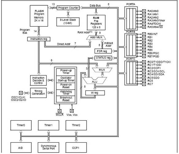
PIC Architecture: PIC controllers are roughly classified by Microchip into three groups: baseline,mid-range, and high-performance. Within each of the groups the PICs are classified based on the first two digits of the PIC’s family type. However, the subclassification is not very strict, since there is some overlap. For this reason we find PICs with 16X designations that belong to the baseline family and others that belong to the mid-range group. In the following subsections we describe the basic characteristics of the various subgroups of the three major PIC families with 8-bit architectures.
Standard features of the PIC
8 bit data path and ALU
Only 35 single word instructions to learn
All single cycle instructions except for program branches, which are two-cycle.
Operating speed: DC-20 MHZ clock input
DC-200 ns instruction cycle
Up to 2k x 14 words of program Memory,
Up to 128 x 8 bytes of Data Memory (RAM)
Pinout compatible to PIC 16C72/72A and PIC 16F872.
Interrupt capability.
Eight- level deep hard ware stack.
Direct, Indirect and Relative Addressing modes.
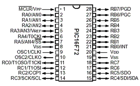
Pin configuration:
PIN DESCRIPTION: MCLR/VPP: Master Clear (Reset) input or programming voltage input. This pin is an active low RESET to the device. RA0 - RA5: These are the bi-directional Input / output PORTA pins. RA1, RA2, are the analog inputs 1, analog input2. RA3 can also be analog input3 or analog reference voltage. RA4 can also be the clock input to the Timer0 module. Output is open drain type. RA5 can also be analog input4 or the slave select for the synchronous serial port. VSS: Ground reference for logic and I/O pins. OSC1/CLK1: Oscillator crystal input / External clock source input. OSC2/CLKO: Oscillator crystal output. Connects to crystal or resonator in Crystal Oscillator mode. In RC mode, the OSC2 pin outputs CLKO, which has 1/4 the frequency of OSC1, and denotes the instruction cycle rate. RC0 – RC7: These are the bidirectional Input / Output PORTC pins. RC0/T1OSO/ T1CK. RC0 can also be the Timer1 oscillator output or Timer1 Clock input. RC1/T1OSI is the Timer1 oscillator input. RC2/CCP is the Capture1 input/Compare1 output/ PWM1 output. RC3/SCK/SCL. RC3 can also be the synchronous serial clock input/output for Both SPI and I2C modes. RC4/SDI/SDA is the SPI Data In (SPI mode) or Data I/O (I2C mode). RC5/SDO is e the SPI Data Out (SPI mode). RC6 RC7. VDD: Positive supply for logic and I/O pins. RB0 – RB7: These are the bi-directional I/O PORTB pins. PORTB can be software programmed for internal weak pull-up on all inputs. RB0/IN is the external interrupt pin. RB1, RB2, RB3 are the bi-directional pins. RB4 is the Interrupt-on-change pin. RB5 is the Interrupt-on-change pin. RB6/PGC is the Interrupt-on-change pin. Serial programming clock. RB7/PGD is the Interrupt-on-change pin. Serial programming data.