ARM basic programming tutorial: In the following ARM processor tutorial i used books to learn fundamental knowledge about Embedded system. The ARM processor core is a key component of many successful 32-bit embedded systems.You probably own one yourself and may not even realize it! ARM cores are widely used in mobile phones, handheld organizers, and a multitude of other everyday portable consumer devices.
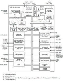
LPC2148(ARM7) Introduction: The LPC2148 microcontrollers is based on a 32-bit ARM7TDMI-S CPU with real-time emulation and embedded trace support, that combine microcontrollers with embedded high-speed flash memory ranging from 32 kB to 512 kB. A 128-bit wide memory interface and unique accelerator architecture enable 32-bit code execution at the maximum clock rate. For critical code size applications, the alternative 16-bit Thumb mode reduces code by more than 30 % with minimal performance penalty. Due to their tiny size and low power consumption, LPC2141/42/44/46/48 are ideal for applications where miniaturization is a key requirement, such as access control and point-of-sale. Serial communications interfaces ranging from a USB 2.0 Full-speed device, multiple UARTs, SPI, SSP to I2C-bus and on-chip SRAM of 8 kB up to 40 kB, make these devices very well suited for communication gateways and protocol converters, soft modems, voice recognition and low end imaging, providing both large buffer size and high processing power. Various 32-bit timers, single or dual 10-bit ADCs, 10-bit DAC, PWM channels and 45 fast GPIO lines with up to nine edge or level sensitive external interrupt pins make these microcontrollers suitable for industrial control and medical systems.
KEY FEATURES OF LPC2148(ARM7) ARCHITECTURE:
16-bit/32-bit ARM7TDMI-S microcontroller in a tiny LQFP64 package.
8 kB to 40 kB of on-chip static RAM and 32 kB to 512 kB of on-chip flash memory; 128-bit wide interface/accelerator enables high-speed 60 MHz operation.
In-System Programming/In-Application Programming (ISP/IAP) via on-chip boot loader software, single flash sector or full chip erase in 400 ms and programming of 256 B in 1 ms.
Embedded ICE RT and Embedded Trace interfaces offer real-time debugging with the on-chip Real Monitor software and high-speed tracing of instruction execution
USB 2.0 Full-speed compliant device controller with 2 kB of endpoint RAM
In addition, the LPC2146/48 provides 8 kB of on-chip RAM accessible to USB by DMA
One or two (LPC2141/42 vs, LPC2144/46/48) 10-bit ADCs provide a total of 6/14 analog inputs, with conversion times as low as 2.44 ms per channel Single 10-bit DAC provides variable analog output (LPC2142/44/46/48 only)
Two 32-bit timers/external event counters (with four capture and four compare
channels each), PWM unit (six outputs) and watchdog.
Low power Real-Time Clock (RTC) with independent power and 32 kHz clock input
Multiple serial interfaces including two UARTs (16C550), two Fast I2C-bus (400 kbit/s),
SPI and SSP with buffering and variable data length capabilities
Vectored Interrupt Controller (VIC) with configurable priorities and vector addresses
Up to 45 of 5 V tolerant fast general purpose I/O pins in a tiny LQFP64 package
Up to 21 external interrupt pins available
60 MHz maximum CPU clock available from programmable on-chip PLL with settling
time of 100 ms
On-chip integrated oscillator operates with an external crystal from 1 MHz to 25 MHz
Power saving modes include Idle and Power-down
Individual enable/disable of peripheral functions as well as peripheral clock scaling for additional power optimization
Processor wake-up from Power-down mode via external interrupt or BOD.
Single power supply chip with POR and BOD circuits.
CPU operating voltage range of 3.0 V to 3.6 V (3.3 V ± 10 %) with 5 V tolerant I/O pads.
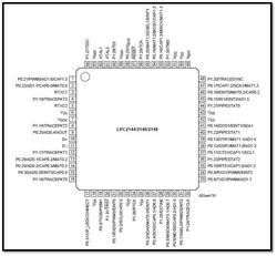
Pin configuration:
PIN DESCRIPTION: P0.0 to P0.31 I/O Port 0: Port 0 is a 32-bit I/O port with individual direction controls for each bit. Total of 31 pins of the Port 0 can be used as a general purpose bidirectional digital I/Os while P0.31 is output only pin. The operation of port 0 pins depends upon the pin function selected via the pin connect block.
P0.0/TXD0/PWM1: P0.0 — General purpose input/output digital pin (GPIO) TXD0 — Transmitter output for UART0 PWM1 — Pulse Width Modulator output 1 P0.1/RXD0/PWM3/EINT0: P0.1 — General purpose input/output digital pin (GPIO) RXD0 — Receiver input for UART0 PWM3 — Pulse Width Modulator output 3 EINT0 — External interrupt 0 input P0.2/SCL0/ CAP0.0: P0.2 — General purpose input/output digital pin (GPIO) SCL0 — I2C0 clock input/output, open-drain output (for I2C-bus compliance) CAP0.0 — Capture input for Timer 0, channel 0 P0.3/SDA0/ MAT0.0/EINT1: P0.3 — General purpose input/output digital pin (GPIO) SDA0 — I2C0 data input/output, open-drain output (for I2C-bus compliance) MAT0.0 — Match output for Timer 0, channel 0 EINT1 — External interrupt 1 input P0.4/SCK0/ CAP0.1/AD0.6 P0.4 — General purpose input/output digital pin (GPIO) SCK0 — Serial clock for SPI0, SPI clock output from master or input to slave CAP0.1 — Capture input for Timer 0, channel 0 AD0.6 — ADC 0, input 6. P0.5/MISO0/ MAT0.1/AD0.7 P0.5 — General purpose input/output digital pin (GPIO) MISO0 — Master In Slave OUT for SPI0, data input to SPI master or data output from SPI slave. MAT0.1 — Match output for Timer 0, channel 1 AD0.7 — ADC 0, input 7 P0.6/MOSI0/ CAP0.2/AD1.0 P0.6 — General purpose input/output digital pin (GPIO) MOSI0 — Master out Slave In for SPI0, data output from SPI master or data Input to SPI slave CAP0.2 — Capture input for Timer 0, channel 2 AD1.0 — ADC 1, input 0, available in LPC2144/46/48 only
P0.7/SSEL0/PWM2/EINT2 P0.7 — General purpose input/output digital pin (GPIO) SSEL0 — Slave Select for SPI0, selects the SPI interface as a slave PWM2 — Pulse Width Modulator output 2 EINT2 — External interrupt 2 input P0.8/TXD1/PWM4/AD1.1 P0.8 — General purpose input/output digital pin (GPIO) TXD1 — Transmitter output for UART1 PWM4 — Pulse Width Modulator output 4 AD1.1 — ADC 1, input 1, available in LPC2144/46/48 only P0.9/RXD1/ PWM6/EINT3: P0.9 — General purpose input/output digital pin (GPIO) RXD1 — Receiver input for UART1 PWM6 — Pulse Width Modulator output 6 EINT3 — External interrupt 3 input P0.10/RTS1/ CAP1.0/AD1.2: P0.10 — General purpose input/output digital pin (GPIO) RTS1 — Request to send output for UART1, LPC2144/46/48 only CAP1.0 — Capture input for Timer 1, channel 0 AD1.2 — ADC 1, input 2, available in LPC2144/46/48 only P0.11/CTS1/ CAP1.1/SCL1: P0.11 — General purpose input/output digital pin (GPIO) CTS1 — Clear to send input for UART1, available in LPC2144/46/48 only CAP1.1 — Capture input for Timer 1, channel 1 SCL1 — I2C1 clock input/output, open-drain output (for I2C-bus compliance)
P0.12/DSR1/MAT1.0/AD1.3: P0.12 — General purpose input/output digital pin (GPIO) DSR1 — Data Set Ready input for UART1, available in LPC2144/46/48 only MAT1.0 — Match output for Timer 1, channel 0 AD1.3 — ADC input 3, available in LPC2144/46/48 only
P0.13/DTR1/ MAT1.1/AD1.4: P0.13 — General purpose input/output digital pin (GPIO) DTR1 — Data Terminal Ready output for UART1, LPC2144/46/48 only MAT1.1 — Match output for Timer 1, channel 1 AD1.4 — ADC input 4, available in LPC2144/46/48 only
P0.14/DCD1/EINT1/SDA1: P0.14 — General purpose input/output digital pin (GPIO) DCD1 — Data Carrier Detect input for UART1, LPC2144/46/48 only EINT1 — External interrupt 1 input SDA1 — I2C1 data input/output, open-drain output (for I2C-bus compliance LOW on this pin while RESET is LOW forces on-chip boot loader to take over control of the part after reset
P0.15/RI1/ EINT2/AD1.5: P0.15 — General purpose input/output digital pin (GPIO) RI1 — Ring Indicator input for UART1, available in LPC2144/46/48 only EINT2 — External interrupt 2 input AD1.5 — ADC 1, input 5, available in LPC2144/46/48 only P0.16/EINT0/MAT0.2/CAP0.2: P0.16 — General purpose input/output digital pin (GPIO) EINT0 — External interrupt 0 input MAT0.2 — Match output for Timer 0, channel 2 CAP0.2 — Capture input for Timer 0, channel 2 P0.17/CAP1.2/ SCK1/MAT1.2: P0.17 — General purpose input/output digital pin (GPIO) CAP1.2 — Capture input for Timer 1, channel 2 SCK1 — Serial Clock for SSP, clock output from master or input to slave MAT1.2 — Match output for Timer 1, channel 2 P0.18/CAP1.3/MISO1/MAT1.3: P0.18 — General purpose input/output digital pin (GPIO) CAP1.3 — Capture input for Timer 1, channel 3 MISO1 — Master In Slave Out for SSP, data input to SPI master or data output from SSP slave MAT1.3 — Match output for Timer 1, channel 3
P0.19/MAT1.2/MOSI1/CAP1.2: P0.19 — General purpose input/output digital pin (GPIO) MAT1.2 — Match output for Timer 1, channel 2 MOSI1 — Master out Slave In for SSP, data output from SSP master or data Input to SSP slave CAP1.2 — Capture input for Timer 1, channel 2 P0.20/MAT1.3/SSEL1/EINT3: P0.20 — General purpose input/output digital pin (GPIO) MAT1.3 — Match output for Timer 1, channel 3 SSEL1 — Slave Select for SSP, selects the SSP interface as a slave EINT3 — External interrupt 3 input P0.21/PWM5/AD1.6/CAP1.3: P0.21 — General purpose input/output digital pin (GPIO) PWM5 — Pulse Width Modulator output 5 AD1.6 — ADC 1, input 6, available in LPC2144/46/48 only CAP1.3 — Capture input for Timer 1, channel 3 P0.22/AD1.7/CAP0.0/MAT0.0: P0.22 — General purpose input/output digital pin (GPIO) AD1.7 — ADC 1, input 7, available in LPC2144/46/48 only CAP0.0 — Capture input for Timer 0, channel 0 MAT0.0 — Match output for Timer 0, channel 0 P0.23/VBUS: P0.23 — General purpose input/output digital pin (GPIO) VBUS — Indicates the presence of USB bus power This signal must be HIGH for USB reset to occur P0.25/AD0.4/AOUT: P0.25 — General purpose input/output digital pin (GPIO) AD0.4 — ADC 0, input 4 AOUT — DAC output, available in LPC2142/44/46/48 only P0.28/AD0.1/CAP0.2/MAT0.2: P0.28 — General purpose input/output digital pin (GPIO) AD0.1 — ADC 0, input 1 CAP0.2 — Capture input for Timer 0, channel 2 MAT0.2 — Match output for Timer 0, channel 2
P0.29/AD0.2/CAP0.3/MAT0.3: P0.29 — General purpose input/output digital pin (GPIO) AD0.2 — ADC 0, input 2 CAP0.3 — Capture input for Timer 0, Channel 3 MAT0.3 — Match output for Timer 0, channel 3 P0.30/AD0.3/EINT3/CAP0.0: P0.30 — General purpose input/output digital pin (GPIO) AD0.3 — ADC 0, input 3 EINT3 — External interrupt 3 input CAP0.0 — Capture input for Timer 0, channel 0 P0.31/UP_LED/CONNECT P0.31 — General purpose output only digital pin (GPO) UP_LED — USB Good Link LED indicator, it is LOW when device is configured (non-control endpoints enabled), it is HIGH when the device is not configured or during global suspend CONNECT — Signal used to switch an external 1.5 kohms resistor under the Software control, used with the Soft Connect USB feature Important: This is a digital output only pin, this pin MUST NOT be externally pulled LOW when RESET pin is LOW or the JTAG port will be disabled P1.0 to P1.31 I/O Port 1: Port 1 is a 32-bit bidirectional I/O port with individual direction controls for each bit, the operation of port 1 pins depends upon the pin function selected via the pin connect block, pins 0 through 15 of port 1 are not Available. P1.16/TRACEPKT0 P1.16 — General purpose input/output digital pin (GPIO) TRACEPKT0 — Trace Packet, bit 0, standard I/O port with internal pull-up P1.17/TRACEPKT1 P1.17 — General purpose input/output digital pin (GPIO) TRACEPKT1 — Trace Packet, bit 1, standard I/O port with internal pull-up P1.18/TRACEPKT2 P1.18 — General purpose input/output digital pin (GPIO) TRACEPKT2 — Trace Packet, bit 2, standard I/O port with internal pull-up P1.19/TRACEPKT3 P1.19 — General purpose input/output digital pin (GPIO) TRACEPKT3 — Trace Packet, bit 3, standard I/O port with internal pull-up P1.20/TRACESYNC P1.20 — General purpose input/output digital pin (GPIO) TRACESYNC — Trace Synchronization, standard I/O port with internal pull-up P1.21/PIPESTAT0 P1.21 — General purpose input/output digital pin (GPIO) PIPESTAT0 — Pipeline Status, bit 0, standard I/O port with internal pull-up P1.22/PIPESTAT1 P1.22 — General purpose input/output digital pin (GPIO) PIPESTAT1 — Pipeline Status, bit 1, standard I/O port with internal pull-up P1.23/PIPESTAT2 P1.23 — General purpose input/output digital pin (GPIO) PIPESTAT2 — Pipeline Status, bit 2, standard I/O port with internal pull-up P1.24/TRACECLK P1.24 — General purpose input/output digital pin (GPIO) TRACECLK — Trace Clock, standard I/O port with internal pull-up P1.25/EXTIN0 P1.25 — General purpose input/output digital pin (GPIO) EXTIN0 — External Trigger Input, standard I/O with internal pull-up P1.26/RTCK P1.26 — General purpose input/output digital pin (GPIO) RTCK — Returned Test Clock output, extra signal added to the JTAG port, assists debugger synchronization when processor frequency varies, bidirectional pin with internal pull-up P1.27/TDO P1.27 — General purpose input/output digital pin (GPIO) TDO — Test Data out for JTAG interface P1.28/TDI P1.28 — General purpose input/output digital pin (GPIO) TDI — Test Data in for JTAG interface P1.29/TCK P1.29 — General purpose input/output digital pin (GPIO) TCK — Test Clock for JTAG interface P1.30/TMS P1.30 — General purpose input/output digital pin (GPIO) TMS — Test Mode Select for JTAG interface P1.31/TRST P1.31 — General purpose input/output digital pin (GPIO) TRST — Test Reset for JTAG interface D+: USB bidirectional D+ line D- : USB bidirectional D- line
RESET External reset input: A LOW on this pin resets the device, causing I/O ports and peripherals to take on their default states, and processor execution to begin at address 0, TTL with hysteretic, 5 V tolerant XTAL1: Input to the oscillator circuit and internal clock generator circuits XTAL2: Output from the oscillator amplifier RTCX1: I Input to the RTC oscillator circuit RTCX2: Output from the RTC oscillator circuit VSS: 6, 18, 25, 42, 50 pins are for supply voltage. Ground: 0 V reference. VSSA Analog ground: 0 V reference, this should nominally be the same voltage as VSS, but should be isolated to minimize noise and error VDD 23, 43, 51 I 3.3 V power supply: This is the power supply voltage for the core and I/O ports. VDDA 7 I Analog 3.3 V power supply: This should be nominally the same voltage as VDD but should be isolated to minimize noise and error, this voltage is only used to power the on-chip ADC(s) and DAC VREF ADC reference voltage: This should be nominally less than or equal to the VDD voltage but should be isolated to minimize noise and error, level on this Pin is used as a reference for ADC(s) and DAC VBAT RTC power supply voltage: 3.3 V on this pin supplies the power to the RTC.